

Modern mobility devices demand a constant balancing act: adding capability without adding size, weight, or power draw. Canted coil springs, however, offer a simple mechanical answer to problems that might otherwise require bulkier, power-hungry systems. This article explores how they support SWaP goals across mobility device design.
Canted Coil Springs
A canted coil spring is a type of coiled spring where the individual coils are tilted (canted) at an angle relative to the spring’s axis, rather than sitting perpendicular to it as in a standard coil spring. Unlike most conventional springs, canted coil springs are also wound with an elliptical (oval), rather than round, cross-section, which is a structural detail that, combined with the coil angle, produces their signature load-deflection behavior.
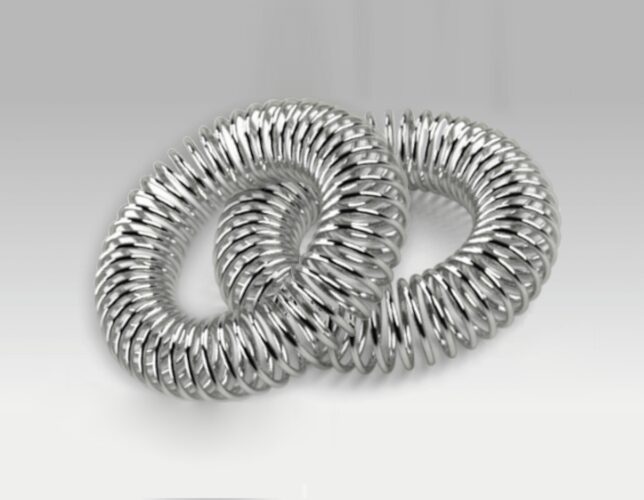
Canted geometry gives these springs a distinctive load-deflection curve: they can provide a nearly constant force over a wide range of deflection. This is unlike conventional springs, where force rises roughly linearly with compression. Because each coil deflects independently, the spring also compensates for wear, misalignment, and tolerance stack-up over its service life rather than losing contact force as mating surfaces change.
Because of this near-constant-force property, their ability to conform to irregular surfaces, and their independent-coil construction, canted coil springs are widely used for fastening and latching, electrical connectors, and EMI shielding. They’re typically manufactured in 300-series stainless steel, Hastelloy, Inconel, Elgiloy, or copper alloys, with Elgiloy generally specified where extreme temperatures or corrosive media are a factor, and can be gold-, silver-, or nickel-plated for electrical or semiconductor applications.
SWaP and Mobility
SWaP stands for Size (or Space), Weight, and Power, three critical constraints engineers must optimize when designing modern electronic and mechanical systems, including mobility devices.
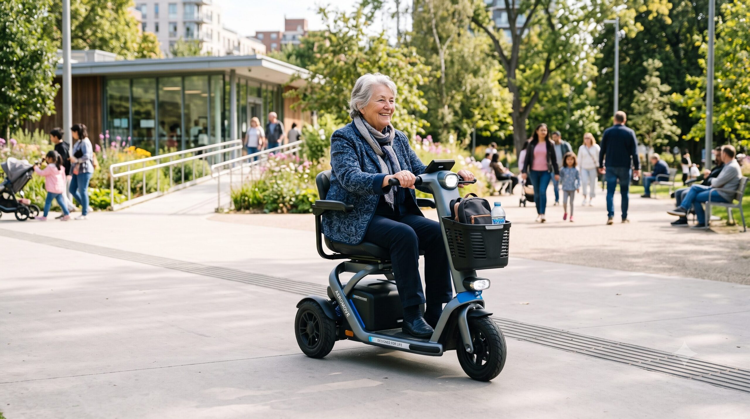
A mobility device is any tool or piece of equipment engineered to help someone move around, maintain balance, or perform physical activities they would otherwise have difficulty with due to injury, disability, illness, or age-related limitations. There are a wide variety of such devices, including canes, crutches, walkers, wheelchairs (manual and powered), mobility scooters, gait trainers, and stairlifts.
For mobility devices, optimizing SWaP means engineers are working to build lighter, more compact equipment that maximizes battery life and maneuverability without sacrificing performance.
Canted Coil Springs and SWaP
Canted coil springs, which feature individual coils set at a slanted angle, are versatile components that may help reduce size, weight, and/or power draw in certain mobility-device subassemblies. The examples below are candidate applications based on the springs’ established engineering behavior. They illustrate where the technology’s known strengths are likely to translate well to mobility hardware, not documented case studies specific to this market.
Impact on Size
Canted coil springs support the Size constraint in SWaP because their compact radial cross-section can deliver meaningful force in a much smaller envelope than many conventional springs or actuators. They can also be integrated directly into joints, connectors, or latch mechanisms without a separate housing.
Candidate applications include compact latch mechanisms for folding wheelchair frames or walkers, where available hardware space is highly constrained; miniature multi-point electrical contacts in joystick-style controllers; space-constrained connector interfaces between battery packs and drive systems in mobility aids; and small-envelope detent mechanisms for adjustable cane or crutch height-locking pins.
Impact on Weight
Canted coil spring solutions are lightweight (and generally less complex) compared to hydraulic or motor-driven mechanisms that might otherwise be needed to achieve similar constant-force behavior.
There are several candidate applications where canted coil springs could help reduce weight. As the detent element in a stepped seat-back recline lock for manual wheelchairs, a canted coil spring could provide reliable, wear-compensating engagement at each locking position. This is a lighter-weight alternative to a heavier ratchet mechanism, though a spring alone is not a substitute for a hydraulic damper where controlled, velocity-dependent recline motion is required for safety.
Canted coil springs may also be well suited as the detent spring in wheelchair quick-release axles, where their independent-coil design could better compensate for wear and tolerance changes over repeated cycles than a conventional single coil spring, improving reliability without adding weight or part count. Finally, they can provide lightweight EMI shielding in onboard electronics for power scooters, potentially replacing heavier shielding gaskets.
Impact on Power
Canted coil springs are purely mechanical, passive components: they draw no power of their own. In electrical-contact applications, such as spring-energized connector contacts between battery and motor interfaces, the only associated loss is minor resistive (I²R) loss at the contact interface, which is negligible compared to the power draw of an active switching or motor-driven alternative. Because the constant-force characteristic requires no active control system or feedback loop to maintain consistent pressure or engagement, canted coil springs can serve locking mechanisms, seating adjustments, and connector contacts without consuming any of a device’s power budget.
Because of this, canted coil springs can enable passive constant-force seating-pressure adjustment, avoiding motorized actuators in cushioning systems. They can also support mechanical (non-electric) locking pins for folding walkers and rollators, preserving battery life for onboard electronics. As spring-energized electrical connector contacts in battery-to-motor interfaces, they maintain reliable contact without active control circuitry. And when used as passive brake or wheel-lock engagement springs in manual wheelchairs, they require no power source to maintain holding force.
There’s also an indirect power benefit: because canted coil solutions are lighter than the hydraulic or motorized systems they can replace, they reduce the overall mass a powered mobility device has to move to improve battery efficiency and range.
Secondary SWaP-Adjacent Benefits
The ability of canted coil springs to conform to irregular or moving surfaces reduces the need for precision-machined mating parts, simplifying manufacturing and reducing part count. Their independent-coil design also means individual coils continue to compensate for wear and misalignment throughout the product’s service life, which can reduce the maintenance burden in applications like wheelchair wheel-lock and brake engagement points.
This durability is directly tied to material selection: canted coil springs made from 300-series stainless steel, Hastelloy, or Elgiloy are engineered to resist a wide range of temperatures and corrosive or humid conditions, which is relevant for mobility devices such as outdoor scooters and rollators that see regular exposure to the elements.
Conclusion
Canted coil springs can offer a low-complexity way to help meet SWaP objectives. Their passive operation, small footprint, and durable, self-compensating design make them a strong candidate for replacing motorized or hydraulic solutions in specific mobility-device subassemblies (provided the application doesn’t require the velocity-dependent damping or continuously variable control that only an active system can provide). These springs are well worth considering in the next mobility device design. If you’d like to learn more about Advanced EMC FlexForce canted coil springs, contact us today!