Engineers are replacing metal bearings too often or are dealing with corrosion, weight, or lubrication failures. PEEK is a high-performance polymer alternative that is changing bearing design. In this article, we look at what PEEK is, why it performs well in many bearing applications, and where it genuinely makes sense to use it.
What Is PEEK and Why Does It Matter for Bearings?
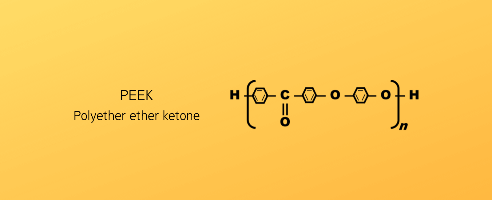
PEEK (Polyether ether ketone) is a semi-crystalline thermoplastic that has proven an excellent solution to many bearing problems. It offers a high strength-to-weight ratio, excellent chemical resistance, a low coefficient of friction, and thermal stability up to 250°C continuous. This combination of properties leads to effective bearing performance, offering PEEK an advantage over both metal and many standard polymer solutions.
High Load Capacity
The standard performance-bearing metric is the PV rating (pressure × velocity). If we look at the PV ratings of commonly used polymer bearing materials, we see that PTFE is severely limited despite its low friction, and nylon and acetal do not do much better. Unfilled PEEK has the best PV ratio, and when filled with carbon fiber, it has a significantly higher PV rating than other engineering polymers. This alone is an excellent reason to consider using PEEK in bearing applications. And note that filled PEEK grades are typically the main choice for demanding applications, while unfilled PEEK is more commonly used where chemical purity or machineability is the priority.
Low Wear Performance
One of the most interesting features of PEEK as a bearing material is its wear resistance, which is critical for many applications. PEEK’s molecular structure resists abrasion under dynamic loading, and it offers excellent performance in dry-running applications because it is self-lubricating, offering an excellent option when lubricants are discouraged or prohibited. Bearing-grade PEEK filled with carbon or graphite further enhances wear performance by significantly reducing wear rates. The low wear performance of PEEK bearings also leads to reduced downtime and longer maintenance intervals.
Where PEEK Bearings Make Sense
PEEK has excellent properties, but they are not an ideal fit for all bearing applications. PEEK bearings are commonly used for applications such as the following:
Medical devices and surgical equipment, where biocompatibility and sterilization resistance prove critical
Food and beverage processing, where the self-lubricating property reduces contamination risks
Aerospace and defense, where the high strength-to-weight ratio leads to weight savings, reduced energy requirements, and SWaP-friendly designs
Chemical processing, where resistance to acids, solvents, and aggressive media exposure is necessary
Semiconductor and cleanroom environments, where PEEK exhibits no outgassing
There are areas where PEEK is not recommended, however. It should not be used in ultra-high load static applications, where steel still dominates. In addition, it’s not well-suited to very high-temperature environments, which are likely beyond PEEK’s thermal ceiling. Finally, PEEK is not a good option for budget-sensitive, low-performance applications where cheaper plastics work well.
Conclusion
PEEK bearings are not a universal replacement for other materials, but rather a viable option for demanding operating environments where their unique properties justify the cost. If you are looking for a sealing solution that sounds like a great application for PEEK, contact the sealing experts here at Advanced EMC and put their knowledge to work for you.
Seals for semiconductor manufacturing involve critical choices related to the material used. And this is not surprising, given the high stakes of semiconductor fabrication, where a single contamination event or seal failure can compromise an entire wafer batch, costing hundreds of thousands of dollars in yield loss.
While seals are small and often overlooked in semiconductor manufacturing, they are exposed to some of the most aggressive conditions imaginable in any industrial environment. However, selecting the right material means not only a reliable seal but also improved equipment uptime, yield, and process integrity.
The Hostile Environment of Semiconductor Manufacturing
There are several factors that contribute to the extremely hostile environment that semiconductor manufacturing seals must be able to withstand. Seals in semiconductor equipment are regularly exposed to acids, bases, solvents, amine-based strippers, and chlorinated gases, depending on the process step.
There is also exposure to plasma: fluorine and oxygen plasmas, commonly used in dry etch and resist stripping, are among the most chemically reactive environments currently known. In addition, plasma exposure will rapidly degrade traditional elastomers that lack full fluorination.
Another challenge lies in extreme temperatures and vacuum pressures. Processes such as CVD (Chemical Vapor Deposition) and LPCVD nitride deposition both demand good thermal stability under sustained high temperatures. Also, many chambers operate under vacuum conditions where outgassing becomes a critical failure mode for the seal material used.
There are also UHP (Ultra-high purity) requirements. In short, any ionic contamination, particulate generation, or elevated TOC (Total Organic Carbon) introduced by a seal can corrupt the process chemistry or inadvertently dope the wafer. This has serious repercussions for semiconductor manufacturing processes and quality.
Seals for Semiconductors: Application-Specific Demands
No single material or seal geometry will work for every process step, so requirements vary significantly by application.
CVD and LPCVD demand thermal stability and vacuum-compatible materials with minimal outgassing. On the other hand, dry and wet etch processes will require a material that is plasma-resistant and compatible with fluorine-based gases and corrosive media.
CMP is especially interesting as it presents a dual challenge: exposure to an abrasive slurry and high-pH chemistry. This necessitates seals with strong abrasion and chemical resistance. Also consider track and lithography equipment that prioritizes solvent resistance, as photoresist developers and solvents readily degrade standard elastomers. Finally, resist stripping adds yet another layer of complexity, requiring seals that can withstand aggressive strip chemistries and sustained ozone exposure.
Plasma resistance, compatibility with fluorine-based gases, and acid/base media
CMP
Abrasive, alkaline slurry exposure
Abrasion resistance, high-pH chemical resistance
Track & Lithography
Photoresist solvent and developer exposure
Broad solvent resistance, dimensional stability
Resist Stripping
Ozone and aggressive strip chemistry exposure
Exceptional chemical resistance, ozone resistance
Material Solutions: Engineering Polymers With Superior Performance
The primary candidate materials for semiconductor manufacturing sealing solutions are polymers selected for their ability to meet the overlapping requirements just described. The engineering polymers discussed are well-adapted to the challenges related to semiconductor manufacturing environments.
FFKM (Perfluoroelastomer)
FFKM is considered the top choice for O-rings in semiconductor manufacturing. It is able to deliver the sealing force and resilience of rubber, but with the chemical compatibility of PTFE. It offers a wide operating temperature, approximately -15°F to 620°F. In addition, there are various grades available for UHP applications that have been optimized for minimal extractable ion content, low metallic contamination, and enhanced O₂/F₂ plasma resistance. FFKM is suitable for static and limited dynamic applications across CVD, CMP, etch, lithography, and stripping processes.
PTFE (Polytetrafluoroethylene)
PTFE is known for its extremely low coefficient of friction, self-lubrication, exceptional chemical compatibility, and high purity. It also performs extremely well in high-temperature, corrosive environments that degrade other material options. Note that PTFE is often the material of choice for highly effective spring-energized seals and reliable encapsulated O-ring jackets.
PEEK (Polyether Ether Ketone)
Like PTFE, PEEK offers good wear resistance and moderate friction properties. It also offers low outgassing, good plasma resistance, and excellent dimensional stability at elevated service temperatures (which can prove crucial). Because of these properties, PEEK is a strong candidate for labyrinth seals and spring-energized seal lips in dynamic semiconductor applications.
Supporting Materials: PI, PCTFE, and PAI (Torlon)
There are some additional supporting materials, namely:
Polyimide (PI): known for its low outgassing, excellent cryogenic performance, and high purity
PCTFE: offers improved strength and hardness over PTFE while retaining excellent chemical inertness
PAI (Torlon): ideal where high pressure, cryogenic temperatures, and corrosive media are all part of the operating environment; known for excellent wear resistance and self-lubrication
Choosing the Right Material
Process
Recommended Materials
Rationale
CVD / LPCVD
FFKM, PEEK, PI (Polyimide)
High thermal stability, low outgassing, vacuum-compatible; FFKM grades available for water vapor and ammonia processes
Dry & Wet Etch
FFKM, PTFE, PCTFE
Superior plasma resistance and broad chemical inertness, including fluorine-based gas compatibility; minimal particle generation
CMP (Chemical Mechanical Polishing)
FFKM, PAI (Torlon), PEEK
Abrasion-resistant with strong resistance to high-pH slurry chemistry; PAI offers excellent wear resistance and self-lubrication
Track & Lithography
FFKM, PTFE, PCTFE
Broad solvent resistance; chemically inert to photoresist solvents and developers that attack standard elastomers
Resist Stripping
FFKM, PTFE
Outstanding ozone resistance and broad chemical compatibility; FFKM specifically rated for ozone and aggressive strip process chemistry
Material selection for semiconductor sealing applications must be matched carefully to the demands of each individual process. For CVD and LPCVD, FFKM, PEEK, and polyimide (PI) are the leading candidates, as all three offer the thermal stability and low outgassing required for sustained high-temperature vacuum operation. Specialized FFKM grades are also available that are formulated specifically for processes involving water vapor and ammonia.
In dry and wet etch environments, FFKM, PTFE, and PCTFE are the materials of choice, owing to their broad chemical inertness and resistance to fluorine-based plasmas and corrosive etch chemistries. Minimal particle generation is a critical secondary requirement in these applications, and all three materials perform well in this regard. For CMP, the combination of abrasive slurry and high-pH chemistry narrows the field to FFKM, PAI (Torlon), and PEEK, with PAI offering a particular advantage due to its exceptional wear resistance and self-lubricating properties.
Track and lithography equipment demands seals that can withstand the photoresist solvents and developers that rapidly degrade conventional elastomers, making FFKM, PTFE, and PCTFE the preferred options given their broad solvent resistance and dimensional stability. Resist stripping represents perhaps the most chemically aggressive environment of all, with ozone exposure compounding an already demanding chemical profile. Here, FFKM and PTFE are the primary recommendations, with select FFKM grades formulated specifically for ozone-intensive strip process chemistry.
Conclusion
In semiconductor manufacturing applications, the seal material selection has an incredible impact on process reliability, contamination control, and total cost of ownership. And there is no universal, one-size-fits-all solution to choosing a seal material. Engineers must look for the optimal combination of material properties to be matched to each process step’s specific chemical, thermal, and purity demands and there are engineering polymers available that are ideal for different applications.
Advanced EMC is your partner when it comes to semiconductor sealing solutions. With over 100 years of combined experience, Advanced EMC has access to UHP-grade FFKM along with a full range of engineered polymer seal type. The Advanced EMC Sealing Solutions Team is ready to identify and supply the right sealing solution for any semiconductor application, whether standard or custom-designed. Contact Advanced EMC today for a consultation or to request a quote.