by Sara McCaslin, PhD Sara McCaslin, PhD No Comments

Meeting SEMI Standards for Seal Purity, Outgassing, and Chemical Resistance

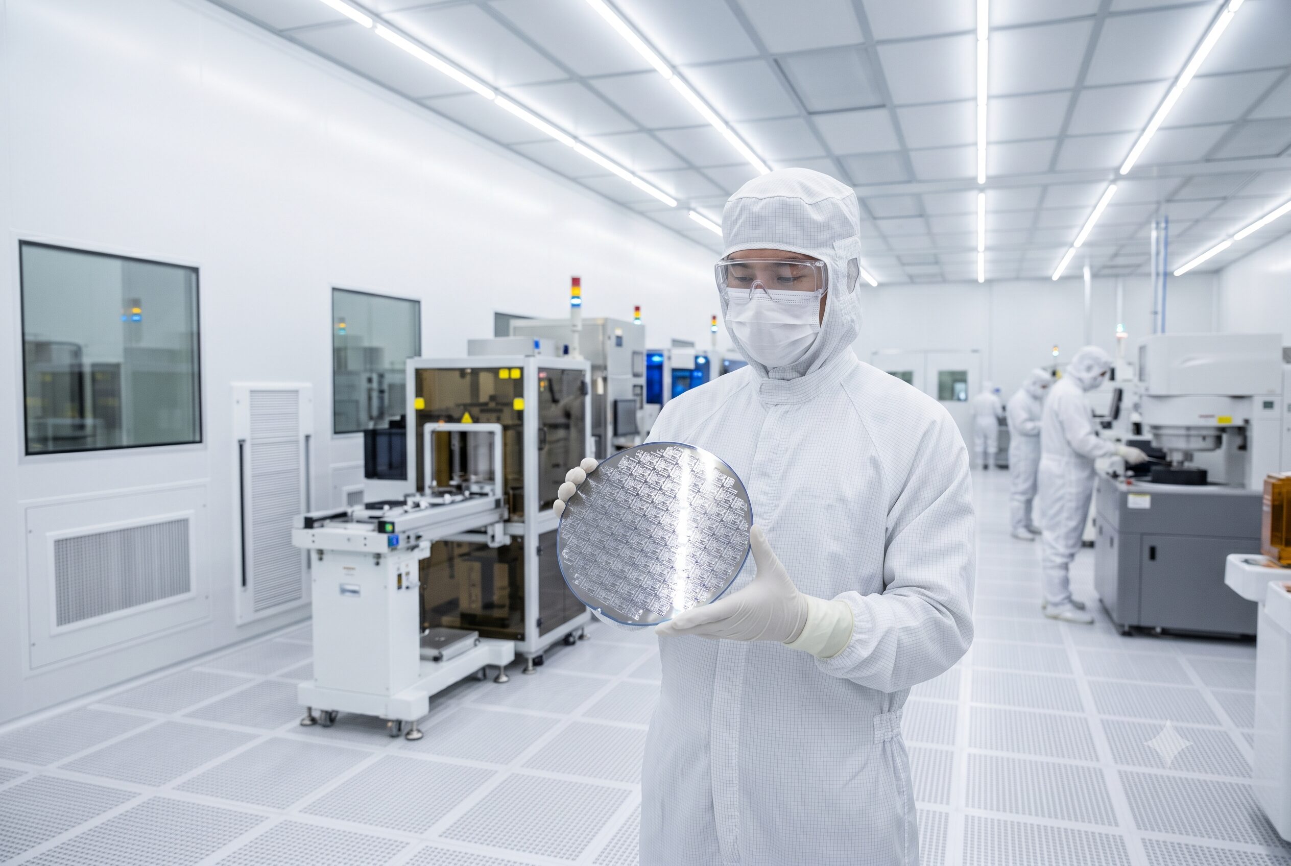
Semiconductor fabrication facilities are among the most demanding environments for seal materials on the planet because a single contamination event can scrap a wafer batch worth hundreds of thousands of dollars. And every polymer, lubricant, and elastomeric material contains residual volatiles. SEMI standards deal with how to take these residual volatiles into account when designing components, such as seals, for wafer fabrication environments. The purpose of this blog post is to discuss what SEMI standards actually require and how engineers select bearings to meet them.

The SEMI Standards Landscape

SEMI standards serve as the common language of the global semiconductor supply chain. For example, SEMI standards define fitness for use by establishing minimum thresholds (e.g., outgassing limits, contamination levels, chemical compatibility requirements) that a component must meet to be considered safe for use in semiconductor manufacturing environments. These standards also protect the wafer from contamination that can destroy device yield and make suppliers accountable. 

By referencing a SEMI standard in a procurement specification, a fabrication engineer can require documented, third-party-verifiable compliance rather than relying on a supplier’s marketing claims. These standards also enable global interoperability: tools, chemicals, and components built to SEMI standards can move across fabrications and geographies without extensive re-qualification. This serves as a major economic benefit in a highly globalized industry.

SEMI F-Series (Facilities and Materials)

The SEMI F-series serves as the most relevant category for seals. Standards like SEMI F57 govern polymeric components and wetted surface materials used in UHP (ultra-high purity) gas distribution systems, covering surface finish requirements, material qualification, and cleanliness protocols. SEMI F2 addresses test methods for metallic contamination on wetted surfaces. These are the specs a seal or bearing supplier is most likely to be asked to demonstrate compliance with.

SEMI C-Series (Chemicals)

The SEMI C-Series of standards defines purity grades and acceptable contamination levels for process chemicals such as acids, solvents, and oxidizers. While these standards primarily govern the chemicals themselves, they are also critically important for material selection. If your seal is sitting in a bath governed by a C-series chemical specification, that specification indirectly defines the chemical resistance your seal must demonstrate. Engineers selecting materials for wetted components need to understand what chemical grade they are designing for.

SEMI S2 (Safety Guidelines for Semiconductor Manufacturing Equipment)

S2 is a broad equipment safety standard with direct implications for materials selection. It addresses chemical containment, materials of construction for chemical-wetted components, ventilation requirements, and labeling. It’s often the standard a tool OEM must satisfy as a condition of fab entry, making it a gateway document that touches bearing and seal design.

Purity: Metallic Contamination and Ionic Cleanliness

When it comes to cleanliness in fabrication environments, the core concern when it comes to contamination is the presence of trace metals (Fe, Na, K, Ca) as killer defects in semiconductor devices. Both dynamic seals are going to shed particles, and this includes wear debris, surface oxides, and manufacturing residues. Among the key material considerations are the use of PTFE bearings and seals, while other options include ceramic bearings (Si₃N₄, ZrO₂) as the go-to for ultra-pure applications and surface treatments (e.g., electropolishing, passivation, and their limits).

Outgassing: The Invisible Contamination Problem

Through outgassing, volatile organic compounds (VOCs) deposit on wafer surfaces and disrupt lithography, deposition, and etch processes. Two standards commonly apply: SEMI F10 and NASA ASTM E595, serving as the benchmarks engineers reference. And there are two key metrics that matter: ML (Total Mass Loss) and CVCM (Collected Volatile Condensable Materials). The general targets used by engineers are TML < 1.0% and CVCM < 0.1%. And remember that a material can pass TML and fail CVCM. Bearings and seals must comply with both. However, CVCM is the one that matters most because it captures what actually re-deposits on a cooler surface.

In seal assemblies, the vast majority of problems come from lubricants and greases (silicone-based greases are particularly problematic in vacuum) and adhesives, polymer cage materials, and elastomeric seals. This includes nylon and acetal bearing cages and standard elastomeric seals with curative that can volatize under heat and vacuum. To avoid these issues, industry best practice is to use …

  • PFPE-based dry film lubricants
  • PTFE lip seals (which are known for their high purity and self-lubrication)
  • Perfluoroelastomers (FFKM)

Bake-Out Procedures

As already discussed, every polymer, lubricant, and elastomeric material contains residual volatiles that may include trapped solvents from manufacturing, absorbed moisture, unreacted monomers, and plasticizer fractions. At room temperature, these substances release slowly over weeks or months. Elevated temperature, however, drives that same process in hours, forcing the material to shed its residual volatiles before it is ever installed. This process is known as bake-out and must be accomplished for a material to be safe to use in a high-purity environment.

Chemical Resistance: Surviving the Process Chemistry

The process chemistry involved with semiconductor manufacturers includes chemicals such as HF, H₂SO₄, HCl, H₂O₂, IPA, NMP, ozone, and aggressive plasma environments. And although a material may be listed as chemically resistant on a data sheet, that does not account for critical variables such as concentration, temperature, and exposure time. Swell, extraction, and stress cracking are the failure modes that tables consistently miss.

The material compatibility hierarchy for seals is:

  • FFKM (Kalrez®, Perlast®): broadest chemical resistance, low extractables
  • PTFE: excellent passive resistance but poor dynamic sealing performance
  • EPDM / FKM (Viton®): acceptable in some applications, disqualified in others (HF is a hard no for FKM)

Conclusion

SEMI compliance is not just a checklist, but rather a systems-level engineering discipline. Material selection, outgassing qualification, and chemical resistance validation must work together to result in a fully SEMI-compliant seal. Engineers who treat these as a system rather than separate line items build better products. If you are looking for a SEMI-compliant sealing solution, contact the engineers at Advanced EMC today.

by Sara McCaslin, PhD Sara McCaslin, PhD No Comments

Seals for Semiconductor Manufacturing 

Seals for semiconductor manufacturing involve critical choices related to the material used. And this is not surprising, given the high stakes of semiconductor fabrication, where a single contamination event or seal failure can compromise an entire wafer batch, costing hundreds of thousands of dollars in yield loss.

While seals are small and often overlooked in semiconductor manufacturing, they are exposed to some of the most aggressive conditions imaginable in any industrial environment. However, selecting the right material means not only a reliable seal but also improved equipment uptime, yield, and process integrity.

The Hostile Environment of Semiconductor Manufacturing

There are several factors that contribute to the extremely hostile environment that semiconductor manufacturing seals must be able to withstand. Seals in semiconductor equipment are regularly exposed to acids, bases, solvents, amine-based strippers, and chlorinated gases, depending on the process step. 

There is also exposure to plasma: fluorine and oxygen plasmas, commonly used in dry etch and resist stripping, are among the most chemically reactive environments currently known. In addition, plasma exposure will rapidly degrade traditional elastomers that lack full fluorination.

Another challenge lies in extreme temperatures and vacuum pressures. Processes such as CVD (Chemical Vapor Deposition) and LPCVD nitride deposition both demand good thermal stability under sustained high temperatures. Also, many chambers operate under vacuum conditions where outgassing becomes a critical failure mode for the seal material used.

There are also UHP (Ultra-high purity) requirements. In short, any ionic contamination, particulate generation, or elevated TOC (Total Organic Carbon) introduced by a seal can corrupt the process chemistry or inadvertently dope the wafer. This has serious repercussions for semiconductor manufacturing processes and quality.

Seals for Semiconductors: Application-Specific Demands

No single material or seal geometry will work for every process step, so requirements vary significantly by application. 

CVD and LPCVD demand thermal stability and vacuum-compatible materials with minimal outgassing. On the other hand, dry and wet etch processes will require a material that is plasma-resistant and compatible with fluorine-based gases and corrosive media. 

CMP is especially interesting as it presents a dual challenge: exposure to an abrasive slurry and high-pH chemistry. This necessitates seals with strong abrasion and chemical resistance. Also consider track and lithography equipment that prioritizes solvent resistance, as photoresist developers and solvents readily degrade standard elastomers. Finally, resist stripping adds yet another layer of complexity, requiring seals that can withstand aggressive strip chemistries and sustained ozone exposure.

ProcessPrimary Sealing ChallengeKey Material Requirements
CVD / LPCVDHigh-temperature vacuum operationThermal stability, vacuum compatibility, minimal outgassing
Dry & Wet EtchHighly aggressive etch chemistriesPlasma resistance, compatibility with fluorine-based gases, and acid/base media
CMPAbrasive, alkaline slurry exposureAbrasion resistance, high-pH chemical resistance
Track & LithographyPhotoresist solvent and developer exposureBroad solvent resistance, dimensional stability
Resist StrippingOzone and aggressive strip chemistry exposureExceptional chemical resistance, ozone resistance

Material Solutions: Engineering Polymers With Superior Performance

The primary candidate materials for semiconductor manufacturing sealing solutions are polymers selected for their ability to meet the overlapping requirements just described. The engineering polymers discussed are well-adapted to the challenges related to semiconductor manufacturing environments. 

FFKM (Perfluoroelastomer)

FFKM is considered the top choice for O-rings in semiconductor manufacturing. It is able to deliver the sealing force and resilience of rubber, but with the chemical compatibility of PTFE. It offers a wide operating temperature, approximately -15°F to 620°F. In addition, there are various grades available for  UHP applications that have been optimized for minimal extractable ion content, low metallic contamination, and enhanced O₂/F₂ plasma resistance. FFKM is suitable for static and limited dynamic applications across CVD, CMP, etch, lithography, and stripping processes.

PTFE (Polytetrafluoroethylene)

PTFE is known for its extremely low coefficient of friction, self-lubrication, exceptional chemical compatibility, and high purity. It also performs extremely well in high-temperature, corrosive environments that degrade other material options. Note that PTFE is often the material of choice for highly effective spring-energized seals and reliable encapsulated O-ring jackets.

PEEK (Polyether Ether Ketone)

Like PTFE, PEEK offers good wear resistance and moderate friction properties. It also offers low outgassing, good plasma resistance, and excellent dimensional stability at elevated service temperatures (which can prove crucial). Because of these properties, PEEK is a strong candidate for labyrinth seals and spring-energized seal lips in dynamic semiconductor applications.

Supporting Materials: PI, PCTFE, and PAI (Torlon)

There are some additional supporting materials, namely:

  • Polyimide (PI): known for its low outgassing, excellent cryogenic performance, and high purity
  • PCTFE: offers improved strength and hardness over PTFE while retaining excellent chemical inertness
  • PAI (Torlon): ideal where high pressure, cryogenic temperatures, and corrosive media are all part of the operating environment; known for excellent wear resistance and self-lubrication

Choosing the Right Material

ProcessRecommended MaterialsRationale
CVD / LPCVDFFKM, PEEK, PI (Polyimide)High thermal stability, low outgassing, vacuum-compatible; FFKM grades available for water vapor and ammonia processes
Dry & Wet EtchFFKM, PTFE, PCTFESuperior plasma resistance and broad chemical inertness, including fluorine-based gas compatibility; minimal particle generation
CMP (Chemical Mechanical Polishing)FFKM, PAI (Torlon), PEEKAbrasion-resistant with strong resistance to high-pH slurry chemistry; PAI offers excellent wear resistance and self-lubrication
Track & LithographyFFKM, PTFE, PCTFEBroad solvent resistance; chemically inert to photoresist solvents and developers that attack standard elastomers
Resist StrippingFFKM, PTFEOutstanding ozone resistance and broad chemical compatibility; FFKM specifically rated for ozone and aggressive strip process chemistry

Material selection for semiconductor sealing applications must be matched carefully to the demands of each individual process. For CVD and LPCVD, FFKM, PEEK, and polyimide (PI) are the leading candidates, as all three offer the thermal stability and low outgassing required for sustained high-temperature vacuum operation. Specialized FFKM grades are also available that are formulated specifically for processes involving water vapor and ammonia.

In dry and wet etch environments, FFKM, PTFE, and PCTFE are the materials of choice, owing to their broad chemical inertness and resistance to fluorine-based plasmas and corrosive etch chemistries. Minimal particle generation is a critical secondary requirement in these applications, and all three materials perform well in this regard. For CMP, the combination of abrasive slurry and high-pH chemistry narrows the field to FFKM, PAI (Torlon), and PEEK, with PAI offering a particular advantage due to its exceptional wear resistance and self-lubricating properties.

Track and lithography equipment demands seals that can withstand the photoresist solvents and developers that rapidly degrade conventional elastomers, making FFKM, PTFE, and PCTFE the preferred options given their broad solvent resistance and dimensional stability. Resist stripping represents perhaps the most chemically aggressive environment of all, with ozone exposure compounding an already demanding chemical profile. Here, FFKM and PTFE are the primary recommendations, with select FFKM grades formulated specifically for ozone-intensive strip process chemistry.

Conclusion

In semiconductor manufacturing applications, the seal material selection has an incredible impact on process reliability, contamination control, and total cost of ownership. And there is no universal, one-size-fits-all solution to choosing a seal material. Engineers must look for the optimal combination of material properties to be matched to each process step’s specific chemical, thermal, and purity demands and there are engineering polymers available that are ideal for different applications.

 Advanced EMC is your partner when it comes to semiconductor sealing solutions. With over 100 years of combined experience, Advanced EMC has access to UHP-grade FFKM along with a full range of engineered polymer seal type. The Advanced EMC Sealing Solutions Team is ready to identify and supply the right sealing solution for any semiconductor application, whether standard or custom-designed. Contact Advanced EMC today for a consultation or to request a quote.