

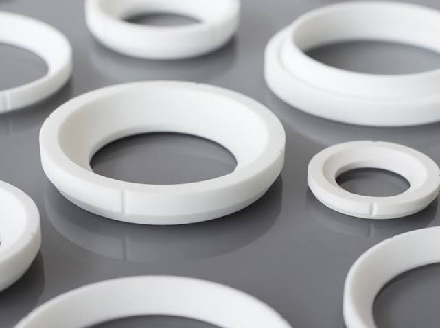
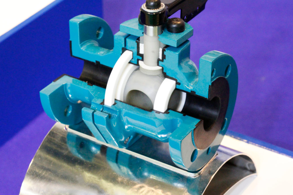
Ball valve seats are critical in industrial fluid control applications. While the valve body and ball are crucial to the design as well, the seat is responsible for sealing the fluid and achieving a uniformly distributed seating stress. That is why poorly specified valve seat materials can lead to leaks, pressure drops, and catastrophic failure.
As an engineer, if you are looking for a reliable seal with a long service life, it is extremely important to match the chemical and mechanical properties of ball valve seats to the specific operating environment, including temperature, pressure, and media compatibility. The objective of this blog post is to review the materials, including their major properties, benefits, and drawbacks, and take a quick look at how to choose the right one.
The Engineering Mechanics and Key Properties of Ball Valve Seats
Soft-seated ball valves depend on the combined elasticity and ductility of polymers to conform to the shape of the ball, leading to a leak-proof seal. As a result, there are some essential material properties that engineers must take into account:
- Low Coefficient of Friction: Low friction will minimize stem torque, which in turn prevents excessive wear and tear that leads to leaks and potentially catastrophic failure.
- Dimensional Stability & Low Thermal Expansion: This combination ensures the seat retains its shape during temperature fluctuations, which is vital for preventing leaks.
- Stress Recovery: Stress recovery is the material’s ability to bounce back (return to its original shape) after continuous cycling and compression.
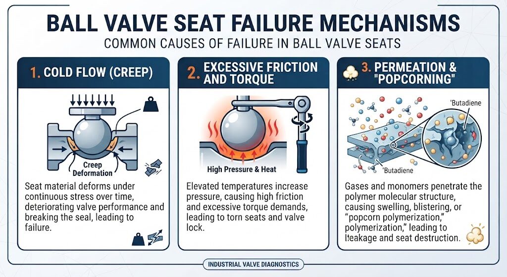
Common Failure Modes Driving Leakage and Lifespan Reduction
There are three common failure modes associated with ball valve seats. These modes drive leakage and lead to a reduced lifespan.
Cold Flow (Creep)
Solid materials slowly deform under continuous mechanical stress in a phenomenon called creep. Over time, this creeping action deteriorates valve performance and breaks the seal. The result is ball valve failure.
Excessive Friction and Torque
Elevated temperatures can increase pressure between the seat and the ball, leading to high friction. High friction leads to higher torque demands, which can ultimately tear the ball valve seats apart and lock the valve.
Permeation and “Popcorning”
Describe how gases and monomers (like butadiene) can penetrate the polymer at a molecular level. Explain how this causes the seat material to swell, blister, or undergo “popcorn polymerization,” leading to catastrophic leakage and seat destruction.
PTFE vs. PEEK for Ball Valve Seats
Two of the most common material choices for ball valve seats are PTFE and PEEK.
Virgin and Filled PTFE (Polytetrafluoroethylene)
Virgin and filled PTFE offer unmatched chemical compatibility, along with the lowest coefficient of friction, self-lubrication, and dry running. They also perform very well in temperatures from cryogenic temperatures down to −330°F up to 400°F–550°F. However, PTFE is highly susceptible to cold creep and radiation damage, so keep in mind that it is not a global solution. At the same time, adding glass or carbon graphite to PTFE not only reduces cold flow but also improves wear and extrusion resistance in high-pressure applications.
PEEK (Polyetheretherketone)
PEEK is another potential option. It has good chemical compatibility, low friction, and self-lubrication combined with excellent mechanical strength and good rigidity. PEEK works extremely well in high-pressure, high-temperature (480°F, continuous and up to 600°F) environments. It’s also unaffected by continuous steam/hot water exposure and is highly resistant to radiation. However, it becomes brittle at low temperatures (making it a poor choice for cryogenic temperatures) and is susceptible to concentrated sulfuric acid and certain highly oxidizing acids. It also requires a higher stem torque than PTFE solutions because its friction, although low, is still higher than PTFE.
Advanced Material Solutions for Niche and Critical Applications
PCTFE (Polychlorotrifluoroethylene)
PCTFE is known for its performance in low-permeation applications. It has a highly dense molecular structure and low microporosity that make it virtually immune to issues with swelling and popcorning. PCTFE maintains mechanical properties down to −400°F, making it ideal for cryogenic applications, and it also works well in semiconductor applications requiring low outgassing. It also exhibits excellent radiation resistance.
TFM (Modified PTFE)
TFM is a second-generation PTFE that offers a much denser molecular structure, allowing it to deliver the chemical resistance of standard PTFE combined with significantly better stress recovery, reduced cold flow, and lower porosity.
Acetal (Delrin) and UHMW-PE
Acetal provides extreme rigidity, high abrasion resistance, and cold flow resistance at pressures up to 5,000 psi and performs quite well in radioactive environments (but should not be used with Oxygen flow). Its primary limitation is its temperature range: −70°F to 180°F. UHMW-PE has specialized low-level radiation resistance and works well with highly abrasive media.
Choosing the Right Material for Ball Valve Seats
| Material | Temp Range | Best For | Watch Out For |
| PTFE (Virgin) | Cryogenic to 400°F | Broadest chemical compatibility, lowest friction | Cold creep, radiation damage |
| PTFE (Filled) | Cryogenic to 550°F | High-pressure service, better wear/extrusion resistance | Slightly less inert than virgin PTFE |
| PEEK | Cryogenic-poor to 600°F | High temp/pressure, steam service, radiation resistance | Brittle when cold, attacked by sulfuric acid |
| PCTFE | Down to -400°F | Cryogenic, low-outgassing (semiconductor) | Niche/higher cost |
| TFM | Same as PTFE | PTFE chemistry with less cold flow/porosity | Premium cost |
| Acetal (Delrin) | Moderate | High-pressure (5,000 psi), abrasion resistance | Narrower chemical range |
| UHMW-PE | General service | Abrasive media, low-level radiation | Not a broad chemical solution |
Conclusion
Moving away from default polymer choices for ball valve seats and moving toward more optimized material choices can result in extended valve life and zero-leakage systems. Remember to specify the polymer compounds used in your design carefully; whether upgrading from virgin PTFE to TFM for better stress recovery, or specifying PCTFE to combat permeation, it can help ensure safety and longevity even in aggressive environments. And if you’d like to talk to one of our sealing specialist engineers, contact Advanced EMC today.